Quick answer
SEM and TEM are both electron microscopy techniques, but they answer different questions. SEM scans the surface of a sample and is usually chosen for surface morphology, topography, particles, coatings, and failure analysis. TEM transmits electrons through a very thin sample and is usually chosen for internal structure, crystal defects, lattice detail, and the highest resolution imaging.
If the main question is "What does the surface look like?", start with SEM. If the main question is "What is happening inside this nanoscale structure?", TEM may be the better method.
Key takeaways
- SEM stands for scanning electron microscopy.
- TEM stands for transmission electron microscopy.
- SEM scans a focused beam across the sample surface.
- TEM sends electrons through an ultrathin sample.
- SEM is usually easier for bulk samples and surface imaging.
- TEM usually offers higher resolution and internal structural information.
- The best choice depends on sample type, feature size, preparation limits, and the scientific question.
SEM vs TEM at a glance
| Feature | SEM | TEM |
|---|---|---|
| Main imaging mode | Scans a beam across the sample | Transmits electrons through the sample |
| Typical information | Surface morphology and composition | Internal structure and crystallography |
| Sample thickness | Bulk or mounted surfaces | Very thin sections or foils |
| Depth of field | High | Lower for thick or complex specimens |
| Resolution potential | High, especially in field emission SEM | Very high, often atomic scale |
| Preparation difficulty | Moderate | Often high |
| Common add-ons | EDX, EBSD, BSE, SE detectors | EDX, EELS, diffraction, STEM modes |
| Typical use | Defects, surfaces, particles, coatings | Lattice detail, interfaces, nanostructure |
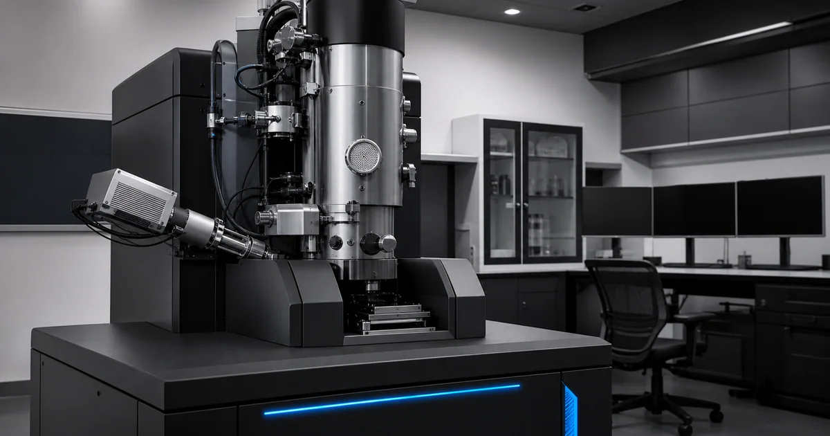
How SEM works
SEM uses a focused electron beam that scans across the sample. Detectors measure signals such as secondary electrons, backscattered electrons, and X-rays. The instrument builds an image from the signal intensity at each beam position.
SEM is excellent for surfaces because many useful signals come from or near the sample surface. This makes SEM practical for fracture surfaces, fibers, powders, insect structures, coatings, corrosion, and manufactured parts.
How TEM works
TEM sends high energy electrons through a very thin sample. The transmitted electrons form an image, diffraction pattern, or analytical signal. Because the electrons pass through the specimen, TEM can reveal internal features that SEM cannot directly show.
TEM is often used for:
- Crystal defects
- Interfaces
- Nanoparticles
- Thin films
- Biological sections
- Lattice fringes
- Phase identification
- Dislocations and grain boundaries
The power of TEM comes with a major requirement: the sample must be thin enough for electrons to transmit through it.
Sample preparation differences
Sample preparation is one of the biggest practical differences between SEM and TEM.
For SEM, a sample may be mounted on a stub, dried, coated, polished, fractured, or sectioned. Many solid samples can be examined with limited preparation. Nonconductive samples may need conductive coating or low vacuum imaging.
For TEM, the sample often needs to be tens to hundreds of nanometers thick, depending on material and accelerating voltage. Preparation may involve ultramicrotomy, ion milling, focused ion beam lift-out, electropolishing, or dispersion onto a support grid.
This difference affects time, cost, sample damage risk, and whether the preparation changes the structure being studied.
Resolution differences
TEM generally provides higher ultimate resolution than SEM. Advanced TEM instruments can image atomic scale structure under suitable conditions.
SEM resolution is still extremely useful. Field emission SEM can resolve fine surface detail at the nanometer scale, especially on well prepared conductive samples. For many industrial and biological questions, SEM resolution is more than enough and the larger field of view is an advantage.
Resolution should not be judged as a single number without context. Useful resolution depends on signal type, sample preparation, contrast, beam damage, vibration, drift, charging, and what feature the user is trying to measure.
Surface information versus internal information
SEM is strongest for surface information. It can show texture, roughness, cracks, pores, particles, fibers, and topographic relationships. Backscattered electron imaging can also show compositional contrast in polished sections.
TEM is strongest for internal information. It can show internal layers, lattice planes, defects, precipitates, and crystallographic relationships. TEM can also use diffraction and spectroscopy to answer structural and chemical questions at very small scales.
EDX in SEM and TEM
Both SEM and TEM can use EDX or EDS for elemental analysis, but the results differ.
In SEM, EDX often samples a larger interaction volume. This is useful for many microanalysis tasks, but it can mix signals from nearby phases or deeper regions.
In TEM, EDX can analyze much smaller regions because the specimen is thin and the probe can be very fine. TEM EDX can be powerful for interfaces and nanoscale particles, but quantification and preparation remain demanding.
When to choose SEM
Choose SEM when you need:
- Surface morphology
- Fracture analysis
- Particle shape and size
- Coating inspection
- Insect, plant, or biological surface detail
- Industrial quality control
- Failure analysis
- Fast survey imaging
- Larger sample compatibility
- SEM EDX microanalysis
SEM is often the first electron microscopy method used because it gives direct visual context quickly.
When to choose TEM
Choose TEM when you need:
- Internal structure
- Crystal defects
- Very high resolution
- Lattice fringes
- Nanoparticle internal detail
- Thin film interfaces
- Electron diffraction
- Nanoscale chemical analysis
- Phase and orientation information at very small scales
TEM is often the right choice when SEM shows that something is interesting, but the answer requires internal nanoscale evidence.
Common mistake: asking which is better
SEM is not simply a weaker TEM, and TEM is not simply a stronger SEM. They are different tools.
SEM gives context, surface form, and practical inspection power. TEM gives internal structure and higher resolution at the cost of more difficult preparation and interpretation.
The better question is: which method best matches the sample and the decision you need to make?
Practical decision guide
Use SEM first if the sample is bulky, the question is surface related, or the goal is fast inspection. Use TEM if the critical feature is internal, nanoscale, crystalline, or too small for SEM to resolve with confidence.
In many research projects, both methods are useful. SEM locates and documents regions of interest. TEM then investigates selected structures in greater depth.