Sections
-

SEM Basics
Plain, accurate introductions to scanning electron microscopy, SEM imaging, resolution, magnification, vacuum, and SEM vs TEM.
Take me to the Basics hub -

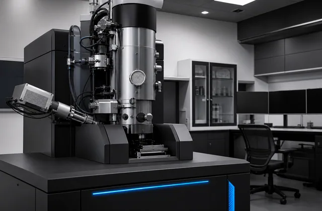
SEM Technology
Instrument architecture and advanced SEM technology for researchers, PhDs, instrument scientists, and lab managers.
Take me to the Technology hub -

SEM Detectors and Signals
Technical resources on secondary electrons, backscattered electrons, in-lens detectors, SE1, SE2, and detector selection.
Take me to the Detectors hub -
SEM Operation Techniques
Practical operating guidance for SEM users: astigmatism, accelerating voltage, detector choice, stage tilt, working distance, and image setup decisions.
Take me to the Operation hub -

EDX, EDS, and EBSD
Elemental analysis and diffraction resources for SEM users, including EDX, EDS, EBSD, mapping, limits, and interpretation.
Take me to the EDX / EDS hub -
SEM Image Atlas
Short scientific articles explaining SEM images of insects, pollen, biological structures, materials, and nanoscale surfaces.
Take me to the Image Atlas hub -

SEM Applications
How SEM is used in materials science, biology, semiconductors, nanotechnology, geology, forensics, batteries, and manufacturing.
Take me to the Applications hub -
SEM Instruments and Buying Guides
Comparison pages for tabletop SEMs, full-size SEMs, lab requirements, used instruments, maintenance, and buying decisions.
Take me to the Instruments hub -
SEM Companies
Corporate overview of SEM vendors, product families, market positions, and buyer research notes.
Take me to the Companies hub -

History of SEM
The development of scanning electron microscopy from early electron optics to modern digital and field-emission instruments.
Take me to the History hub -

SEM News
A running editorial desk for SEM instrument releases, detector advances, AI-assisted microscopy, research highlights, and conference notes.
Take me to the News hub -

SEM Resources
Useful SEM channels, books, courses, glossaries, protocols, and microscopy communities.
Take me to the Resources hub -
SEM Sample Preparation
Future hub for coating, mounting, drying, cryo preparation, biological samples, conductive adhesives, and contamination control.
Take me to the Sample Prep hub -

SEM Troubleshooting
Future hub for charging, contamination, drift, astigmatism, poor signal, beam damage, and EDX artifacts.
Take me to the Troubleshooting hub -

SEM Protocol Library
Future hub for repeatable SEM imaging, EDX, EBSD, biological sample prep, and materials characterization workflows.
Take me to the Protocols hub -

SEM Research Digest
Future hub for readable summaries of SEM-related papers, methods, and application notes.
Take me to the Research Digest hub -
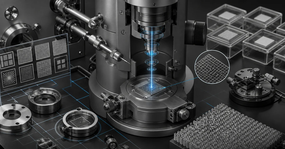
SEM Optics Calibration
Verifying and correcting SEM electron-optical performance against known standards. Magnification calibration with traceable reference samples, resolution verification, aperture and gun alignment procedures, routine calibration workflows.
Take me to the Calibration hub