Subject
SEM Technology
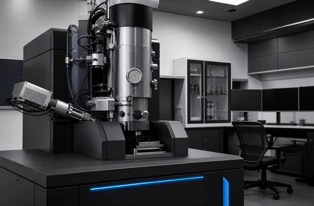
Instrument architecture and advanced SEM technology for researchers, PhDs, instrument scientists, and lab managers.
Quick answer
Advanced scanning electron microscopy is the coordinated use of electron source brightness, column optics, detector strategy, vacuum control, analytical instrumentation, and software automation to answer research questions at micro- and nanoscale length scales.
For PhDs, principal investigators, core facility managers, and industrial research groups, the important question is rarely "Which SEM has the best headline resolution?" A better question is: which SEM can produce interpretable contrast, stable measurements, and reliable analytical data on the actual samples the lab studies every week?
Modern SEM technology is best understood as a system. The electron source determines brightness and energy spread. The column shapes the probe. The sample chamber determines geometry and analytical access. Detectors convert electron and photon signals into image contrast. Vacuum mode affects charging and contamination. Software decides how repeatable and scalable the workflow becomes.
Key takeaways
- Field emission sources usually provide the strongest platform for low-voltage, high-resolution research imaging.
- Tungsten and other thermionic instruments can still be excellent for robust routine imaging and teaching.
- Detector choice can change the scientific interpretation of an SEM image as much as accelerating voltage or working distance.
- Low-kV SEM is central for surfaces, polymers, thin films, biological coatings, and beam-sensitive materials.
- Analytical SEM work depends on geometry, probe current, detector solid angle, standards, calibration, and sample preparation.
- A research SEM should be evaluated with representative samples, not only vendor demonstration specimens.
What advanced SEM technology includes
An advanced SEM is not defined by one feature. It is a platform that gives the operator control over multiple interacting variables.
Electron source:
- Tungsten thermionic filament
- Lanthanum hexaboride, often written as LaB6
- Schottky field emission source
- Cold field emission source
Electron optics:
- Condenser lens system
- Objective lens design
- Apertures
- Stigmators
- Beam deceleration or stage bias
- In-lens or through-the-lens detection paths
Signal detection:
- Secondary electron imaging
- Backscattered electron imaging
- In-lens secondary electron imaging
- Energy dispersive X-ray spectroscopy, also called EDX or EDS
- Electron backscatter diffraction, commonly EBSD
- Cathodoluminescence
- Scanning transmission electron microscopy modes in SEM, often called STEM-in-SEM
Operational environment:
- High vacuum
- Low vacuum
- Variable pressure
- Environmental SEM
- Cryogenic SEM
- Clean transfer or inert transfer workflows
Research performance emerges from how these elements work together.
Electron source and beam quality
The electron source is one of the first decisions that separates routine SEM from advanced SEM.
A tungsten filament is inexpensive, robust, and easy to maintain. It provides enough beam current for many routine imaging tasks, fracture surface studies, teaching labs, and quality control. Its limitations become visible when a researcher needs a very small probe at low accelerating voltage, high brightness for analytical work, or long sessions with minimal drift in beam characteristics.
Field emission sources provide higher brightness and a smaller effective source size. That allows the column to form a finer probe, often with better low-kV performance. A Schottky field emission SEM is common in research facilities because it balances high brightness with operational stability. A cold field emission SEM can offer very high brightness and narrow energy spread, but it may require more demanding vacuum and maintenance practices.
For researchers, beam quality matters because it affects:
- Spatial resolution
- Edge definition
- Low-voltage surface sensitivity
- Probe current at small spot size
- EDX count rate
- EBSD pattern quality
- Beam damage and contamination rate
The same nominal accelerating voltage can behave very differently across instruments if source brightness, column design, and detector layout differ.
Low-voltage SEM and surface sensitivity
Low-voltage SEM is one of the most important areas of modern SEM technology. Imaging at 5 kV, 2 kV, 1 kV, or below can reduce interaction volume, increase surface sensitivity, and limit charging or beam damage. This is especially useful for thin films, polymers, nanoparticles, coatings, biological specimens, battery materials, and semiconductor surfaces.
The tradeoff is signal. At low voltage, probe formation becomes harder, EDX excitation is limited, and some detectors become less efficient. High-end field emission SEMs address this with improved objective lens designs, in-lens detectors, beam deceleration, and optimized signal collection.
Beam deceleration can be especially useful. The column operates at a higher beam energy for better optical performance, while the sample is biased so the landing energy is lower. The result can be improved surface imaging at very low landing energies, although charging, sample geometry, and stage bias safety must be considered.
Detectors define contrast
SEM images are not neutral photographs. They are maps of electron signals. Advanced SEM users choose detectors to isolate the signal that answers the question.
Secondary electron detectors emphasize surface topography and fine edge detail. Backscattered electron detectors emphasize atomic number contrast, phase differences, and compositional variation. In-lens detectors can provide high-resolution surface information, especially at low accelerating voltage. Directional backscatter detectors can reveal channeling, phase contrast, or topographic shading depending on geometry.
This matters for publication-quality interpretation. A particle that appears bright in a backscatter image may be compositionally heavy, not taller. A surface that appears sharp in secondary electron imaging may not reflect subsurface structure. A rough sample imaged at a short working distance may favor one detector and penalize another.
Advanced SEM work should record detector type, accelerating voltage, probe current or spot size, working distance, chamber pressure, coating condition, and sample tilt when those factors affect interpretation.
Analytical SEM: EDX, EBSD, and beyond
Analytical SEM turns the microscope into a microanalysis platform.
EDX identifies elements through characteristic X-rays generated by beam-sample interaction. It is powerful, fast, and widely used, but it has limits. Light elements are harder to quantify, peak overlaps can mislead interpretation, and spatial resolution is constrained by interaction volume. At higher accelerating voltages, X-rays can originate below the apparent surface feature in the image.
EBSD analyzes crystallographic orientation from diffraction patterns produced by a tilted specimen. It is essential in metallurgy, geology, ceramics, additive manufacturing, and semiconductor research. EBSD performance depends on sample preparation, surface quality, detector geometry, beam stability, and pattern indexing software.
Other analytical extensions include wavelength dispersive spectroscopy, cathodoluminescence, time-resolved or in situ stages, and correlative workflows with optical microscopy, FIB, TEM, Raman spectroscopy, or X-ray microscopy.
Vacuum modes and difficult samples
High vacuum gives the cleanest electron path and is the default for many conductive or coated samples. The problem is that many valuable research samples are insulating, hydrated, porous, outgassing, or sensitive to preparation.
Variable pressure SEM introduces gas into the chamber to reduce charging and allow less conductive specimens to be imaged without full conductive coating. Environmental SEM extends this idea further by supporting higher chamber pressures and more complex specimen environments.
These modes open important sample classes, but they are not free upgrades. Gas scattering can reduce resolution. Detector choices change. Beam interactions become more complex. For quantitative analysis, the operator must understand how pressure, working distance, and gas path length influence signal and X-ray detection.
Automation and reproducibility
Advanced SEM is increasingly software-defined. Automated montaging, autofocus, auto-stigmation, recipe-based imaging, stage mapping, feature detection, particle analysis, and AI-assisted segmentation can make a core facility more productive.
For research, automation is valuable when it improves reproducibility rather than merely increasing image volume. A useful automated workflow should record metadata, preserve acquisition parameters, allow review of focus and astigmatism decisions, and export data in formats that support downstream analysis.
Core facilities should ask whether the software supports:
- Repeatable recipes
- Batch acquisition
- Metadata export
- Correlative coordinate systems
- Multi-user permissions
- Audit trails
- Remote operation policies
- Integration with image analysis tools
How to evaluate an advanced SEM
A serious evaluation should use representative specimens from the lab, not only vendor standards.
Recommended test set:
- A conductive high-resolution standard
- A low-kV surface-sensitive sample
- A beam-sensitive polymer or biological specimen
- A rough bulk sample
- A sample requiring EDX
- A sample requiring EBSD if relevant
- A charging-prone uncoated sample
Recommended evaluation questions:
- What resolution is achieved at the voltages the lab actually uses?
- How stable is the image over a long acquisition?
- How often is manual stigmation required?
- Can the microscope switch efficiently between imaging and analysis?
- Does the stage return accurately to stored coordinates?
- How much sample preparation is needed for reliable results?
- What service response and source replacement costs should be expected?
Common mistakes
The most common mistake is buying for the best specification sheet rather than the highest research throughput. A microscope with excellent resolution may still be a poor fit if it has limited chamber access, poor analytical geometry, fragile workflows, or software that slows routine use.
Another mistake is treating EDX, EBSD, and low-vacuum imaging as simple add-ons. Each one changes the practical requirements of the instrument. Analytical work may require more beam current, more stage stability, specific working distances, and careful sample preparation.
Finally, research groups often underestimate training. Advanced SEM capability depends heavily on operator judgment. The best instrument in the room still needs users who understand signal origin, artifacts, charging, contamination, drift, and detector geometry.
Researcher checklist
Before choosing or upgrading an SEM, define:
- Primary sample types
- Required length scale
- Conductivity and preparation limits
- Need for low-kV imaging
- Need for EDX, EBSD, or other analysis
- Expected daily sample volume
- User skill level
- Service and consumable budget
- Data management requirements
The right SEM technology choice is the one that turns difficult specimens into repeatable evidence.
Where to go next
A short editorial reading list. Pick whichever fits how you like to learn.
- Royal Microscopical Society: professional microscopy community and education
- Microscopy Society of America: society resources, meetings, and microscopy community