Quick answer
The history of scanning electron microscopy is the story of turning electron beams into practical surface images.
Early electron microscopes proved that electrons could resolve detail beyond the limits of visible light. SEM added a different idea: scan a focused electron probe across a specimen, collect emitted signals point by point, and build an image from how the sample responds.
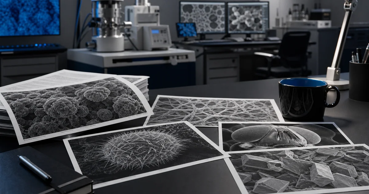
That scanning approach made SEM especially useful for surface structure, fractures, particles, insects, fibers, coatings, semiconductor features, geological grains, and many other specimens where topography matters.
Timeline at a glance
| Period | Development | Why it mattered |
|---|---|---|
| 1920s to 1930s | Electron optics and early electron microscopes | Established that electron beams could be focused and used for imaging |
| 1930s | Scanning concepts and electron probe work | Connected raster scanning with localized sample response |
| 1940s to 1950s | Instrument refinements and research prototypes | Improved beams, detectors, vacuum systems, and image formation |
| 1950s to 1960s | Cambridge SEM research under Charles Oatley | Made SEM more practical for real specimens and real laboratories |
| 1965 | Cambridge Instruments Stereoscan | First major commercial SEM platform |
| 1970s to 1990s | Digital control, better detectors, field emission, EDX integration | Turned SEM into a broad analytical workhorse |
| 2000s to today | FIB-SEM, environmental SEM, automation, AI-assisted workflows | Expanded SEM from imaging into 3D analysis, correlative workflows, and high throughput characterization |
Before SEM: why electrons changed microscopy
Light microscopy is limited by the wavelength of visible light. For many biological and industrial questions, optical microscopes are still ideal. But they cannot directly resolve many nanoscale surface features, thin films, nanoparticles, fracture details, or sub-micron manufacturing defects.
Electron microscopy was a response to that limitation. Electrons can behave as waves with much shorter wavelengths than visible light, which opened a path to higher resolution imaging. Transmission electron microscopy, or TEM, became a major early branch, but TEM usually requires thin specimens and forms images from electrons transmitted through the sample.
SEM solved a different problem. It allowed researchers to inspect surfaces and near-surface signals from bulkier specimens, often with a striking depth of field that made small structures visually understandable.
The scanning idea
The central SEM idea is simple to describe:
- Focus an electron beam into a small probe.
- Move that probe across the specimen in a raster pattern.
- Detect signals generated by beam-sample interaction.
- Convert signal intensity into image brightness at each scanned point.
The practical execution was not simple. SEM required stable electron optics, reliable scanning electronics, usable detectors, vacuum engineering, sample stages, and image display systems. The instrument had to keep the beam controlled while collecting weak signals from a complex interaction volume inside the sample.
Early contributors
SEM history is often told through several linked technical streams rather than one single inventor.
Max Knoll is commonly associated with early electron beam scanning work. Manfred von Ardenne contributed important work on scanning electron and scanning transmission concepts in the 1930s. Vladimir Zworykin and colleagues reported further developments. Later, the Cambridge group led by Charles Oatley helped transform SEM into an instrument that could become commercially viable.
The important point for readers is this: SEM was not a single sudden breakthrough. It was a convergence of electron optics, probe scanning, signal detection, vacuum systems, and practical instrument design.
The Cambridge step
The Cambridge work in the 1950s and early 1960s was decisive because it pushed SEM toward routine usability.
Academic prototypes can prove a principle. A laboratory instrument needs repeatability, serviceability, image quality, and a reason for buyers to prefer it over other methods. The Cambridge program helped develop SEM as a real research instrument for surface study.
That work led into the Cambridge Instruments Stereoscan, introduced in 1965. The Stereoscan is widely cited as the first commercial scanning electron microscope and marks a clear transition from experimental SEM to market adoption.
Why the first commercial SEM mattered
The commercial SEM mattered because it gave laboratories a new kind of image.
SEM images looked different from optical micrographs and TEM images. They had strong apparent depth, high surface detail, and a practical magnification range. For many users, SEM became the fastest way to understand a specimen's surface:
- Is a fracture ductile, brittle, intergranular, or fatigue-related?
- What is the morphology of a powder?
- How are fibers arranged?
- Are particles contaminating a surface?
- What does an insect eye, pollen grain, or diatom look like at micro scale?
- Where should EDX analysis be performed?
The first commercial systems did not have the automation, digital interfaces, or detector variety of modern instruments. But they created the category.
Field emission and higher performance
As SEM matured, one major improvement was the field emission gun, often shortened to FEG.
Compared with conventional thermionic sources, field emission sources can provide a smaller, brighter electron probe. That matters for high resolution imaging, low voltage work, and advanced analytical performance. FEG-SEM systems became important in nanomaterials, semiconductor inspection, coatings, catalysts, ceramics, and high performance materials research.
Thermionic SEM systems did not disappear. Tungsten and LaB6 instruments remain useful for routine imaging, teaching, industrial quality control, and applications where ultimate resolution is not the main requirement.
Detectors made SEM more than an image tool
SEM became more powerful as detector options expanded.
Secondary electron detectors made surface topography visible. Backscattered electron detectors added composition-sensitive contrast because heavier elements generally backscatter electrons more strongly. In-lens and through-lens detectors improved signal collection in some field emission systems. EDX detectors added elemental analysis. EBSD made crystallographic information accessible in properly prepared specimens.
Modern SEM is therefore not just a microscope. It is often a platform for multimodal microanalysis.
Low vacuum, variable pressure, and environmental SEM
Traditional SEM usually requires high vacuum and conductive or coated samples. That creates problems for wet, oily, insulating, charging, or delicate specimens.
Low vacuum, variable pressure, and environmental SEM methods reduced some of those limits. They allow imaging under controlled gas pressure and can help manage charge on nonconductive materials. Environmental SEM can support selected hydrated or pressure-sensitive specimens, depending on the instrument and method.
These modes do not remove all preparation constraints. They do, however, make SEM useful for a wider range of samples.
Digital SEM and modern workflows
Digital control changed SEM operation. Earlier systems required more manual tuning and analog display methods. Modern SEMs use digital scan control, image capture, motorized stages, recipe-based acquisition, automated montaging, live EDX mapping, and software-assisted alignment.
The direction is clear: SEM is moving from a single expert sitting at an instrument toward reproducible workflows that can be shared, audited, and repeated.
That matters for industrial labs, academic core facilities, and regulated environments where documentation is as important as a beautiful image.
FIB-SEM and 3D analysis
Focused ion beam SEM, or FIB-SEM, joined ion milling with SEM imaging. A focused ion beam can remove material in controlled slices while the SEM images the exposed face.
That enables 3D reconstruction of microstructures, site-specific cross sectioning, circuit edit workflows, TEM lamella preparation, battery material analysis, porous media study, and failure analysis.
FIB-SEM is one of the clearest examples of SEM becoming part of a broader analytical workstation rather than a standalone surface camera.
SEM today
Current SEM development is shaped by several pressures:
- Higher throughput for busy facilities.
- Lower voltage imaging for beam-sensitive materials.
- Better detector integration for topography, composition, and crystallography.
- Easier operation for shared labs and teaching environments.
- Better automation for repeatable industrial inspection.
- AI-assisted segmentation, focus, feature detection, and image interpretation.
- Correlative workflows that connect SEM with optical, X-ray, TEM, and spectroscopy data.
SEM remains a mature technology, but it is not static. Its value keeps expanding because the instrument sits at a useful boundary between imaging, measurement, chemistry, structure, and manufacturing.
Key takeaway
Scanning electron microscopy became important because it made tiny surfaces legible.
The method began with electron optics and scanning concepts, became practical through mid-century instrument development, entered the market with the Stereoscan in 1965, and evolved into a family of digital analytical platforms. Today, SEM is one of the core tools for seeing and measuring the micro world.