Quick answer
SEM news is broader than product announcements. A useful scanning electron microscopy digest tracks instruments, detectors, software, sample preparation, analytical workflows, and the research fields that push SEM to do more.
The most important developments usually fall into six areas:
- Higher resolution and better low voltage performance.
- Better detector integration for SE, BSE, EDX, EBSD, STEM-in-SEM, and cathodoluminescence.
- More automation for routine and high throughput labs.
- FIB-SEM expansion for 3D and site-specific workflows.
- AI-assisted image analysis and instrument operation.
- Application pressure from semiconductors, batteries, additive manufacturing, biology, and advanced materials.
Why SEM news matters
Scanning electron microscopy is a mature technique, but the market and research landscape are active.
A new SEM model may matter because it lowers the barrier to high resolution imaging. A detector update may matter because it improves contrast at low voltage. A software release may matter because it makes repeatable image acquisition easier in a shared facility. A research paper may matter because it shows how SEM can answer a question that previously required slower, more destructive, or less accessible methods.
For labs, news is not entertainment. It is planning input.
What SemSip watches
SemSip organizes SEM news into practical editorial categories.
| News area | What to watch | Why it matters |
|---|---|---|
| Instruments | New SEM, FE-SEM, tabletop SEM, low vacuum SEM, and FIB-SEM platforms | Shapes buying decisions and facility planning |
| Detectors | SE, BSE, in-lens, EDX, EBSD, STEM, and cathodoluminescence updates | Changes what contrast and measurements are practical |
| Software | Automation, montaging, recipe workflows, EDX maps, segmentation, and reporting | Improves throughput and reproducibility |
| Sample preparation | Coating, polishing, cryo, plasma cleaning, cross sectioning, and charge control | Determines whether the image is trustworthy |
| Applications | Batteries, semiconductors, insects, biomaterials, polymers, catalysts, powders, and failure analysis | Shows where SEM is gaining new value |
| Research methods | Low voltage SEM, 3D FIB-SEM, correlative microscopy, and AI analysis | Indicates where the field is moving next |
Instrument releases
New SEM models usually emphasize some combination of resolution, ease of use, stability, detector choice, analytical integration, or throughput.
For a publication reader, the key is to separate marketing language from real capability. Useful questions include:
- Does the model improve the work people actually perform?
- Is the quoted resolution relevant at the voltages used for real samples?
- Does the instrument support charge-prone or nonconductive samples?
- Are EDX, EBSD, or other analytical options integrated cleanly?
- Does the software support repeatable recipes and audit-friendly exports?
- Is service coverage strong in the buyer's region?
The best news coverage should translate specifications into consequences.
Detector and signal developments
Detector changes can be more important than column changes for many users.
Secondary electron detectors emphasize topography. Backscattered electron detectors can reveal composition and phase contrast. In-lens detectors can improve surface-sensitive imaging in field emission systems. EDX detects characteristic X-rays for elemental analysis. EBSD can map crystal orientation when the sample is prepared correctly.
When detector news appears, the editorial question is: which specimens become easier to interpret?
For example, an improved BSE detector may help with low kV phase contrast. A faster EDX workflow may help industrial labs screen particles or inclusions. Better EBSD integration may matter for metallurgy, additive manufacturing, and geological samples.
AI in SEM
AI is becoming relevant because SEM data can be abundant, repetitive, and difficult to review by hand.
Potential uses include:
- Segmenting pores, grains, fibers, particles, cells, or fracture features.
- Detecting defects in semiconductor or manufacturing workflows.
- Assisting focus, stigmation, and image quality checks.
- Classifying particles or inclusions using images plus EDX data.
- Supporting high throughput review of large montages.
- Reducing manual reporting burden.
AI does not replace microscopy judgment. SEM images can contain preparation artifacts, charging, contamination, drift, detector bias, and misleading contrast. Any AI result needs validation against sample context and physical understanding.
FIB-SEM and 3D workflows
FIB-SEM remains one of the most important advanced SEM-adjacent areas.
By milling and imaging serial sections, FIB-SEM can reconstruct 3D microstructures. That is valuable for batteries, catalysts, porous materials, failure analysis, microelectronics, coatings, and biological ultrastructure workflows.
News in this area often concerns faster milling, lower damage preparation, larger volume reconstruction, better automation, improved plasma FIB performance, and easier correlation with EDX, EBSD, or TEM sample preparation.
EDX and analytical SEM
EDX, also called EDS, turns SEM from a visual tool into an elemental analysis platform.
Important EDX news includes detector area, count rate, low energy sensitivity, software quantification, map speed, phase analysis, standardless analysis improvements, and reporting tools. The practical question is whether the system gives a faster or more reliable answer for a specific sample.
EDX remains limited by interaction volume, peak overlap, surface contamination, sample geometry, low-Z element detection challenges, and calibration assumptions. Good news coverage should mention those limits.
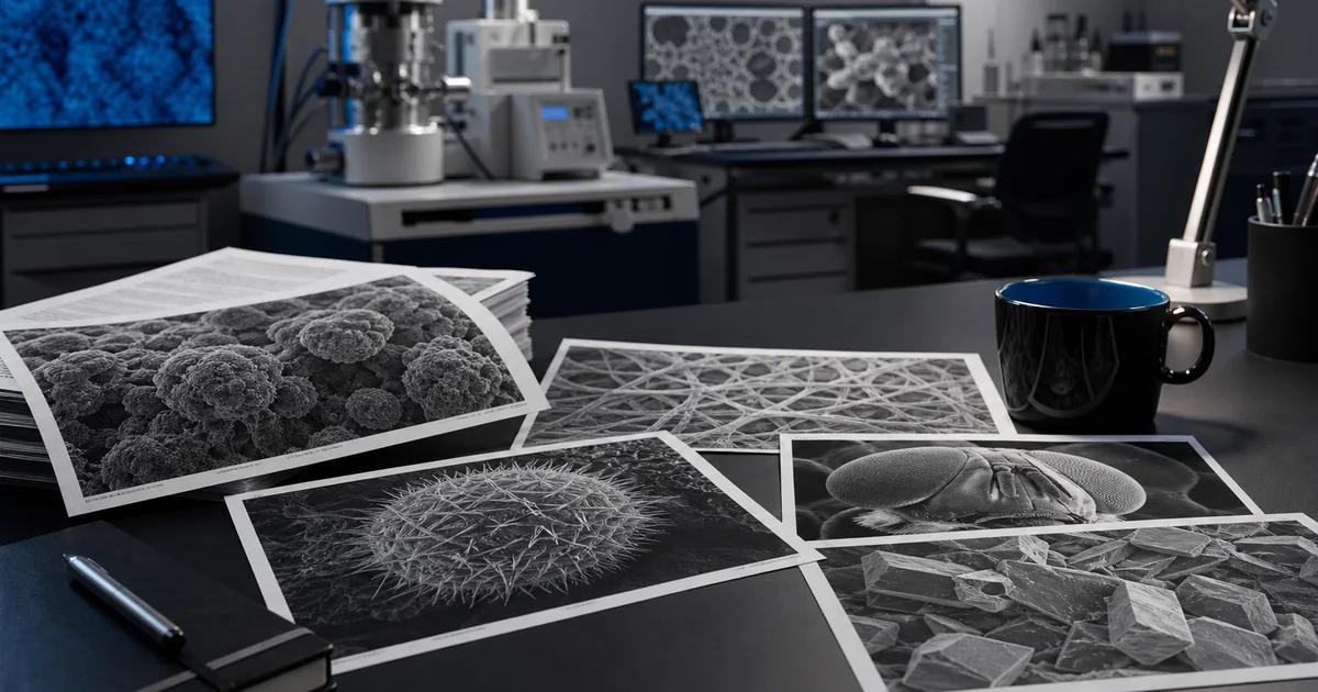
Application areas to watch
Batteries
Battery research uses SEM for electrode morphology, particle cracking, separator structure, coatings, lithium-related degradation studies, and failure analysis. Beam sensitivity and sample preparation are major concerns.
Semiconductors
Semiconductor work uses SEM for defect inspection, critical dimensions, cross sections, failure analysis, and process monitoring. Automation and repeatability are central.
Additive manufacturing
Powder morphology, surface defects, porosity, melt pool structures, fracture surfaces, and inclusions make SEM valuable in additive manufacturing workflows.
Biology and insects
SEM remains visually powerful for surface anatomy: compound eyes, hairs, scales, pollen, mouthparts, wings, and exoskeletons. The preparation method strongly affects interpretation.
Materials failure analysis
Fracture surfaces, corrosion products, wear debris, coatings, inclusions, and particles are classic SEM subjects. SEM plus EDX often provides the first strong clue in an investigation.
How to read SEM news critically
Ask five questions:
- What sample or workflow does this improve?
- Is the evidence a controlled demonstration or a general claim?
- Which detector, voltage, vacuum mode, and preparation method were used?
- Are limitations stated clearly?
- Can an independent lab reproduce the result with normal operators?
News becomes useful when it helps a microscopist decide what to test next.
Key takeaway
The future of SEM is not only sharper images. It is better workflows: stronger detectors, cleaner analysis, easier operation, smarter software, faster throughput, and more reliable interpretation.
SemSip's digest will treat SEM as both an instrument and a knowledge system: what changed, who it helps, what to verify, and what it means for real samples.